Yaping Dan
Silicon Thin Film
Globle Institute of Future Technology (University of Michigan - Shanghai Jiao Tong University Joint Institute), Shanghai Jiao Tong University 200240, Shanghai, China
Email: yaping.dan@sjtu.edu.cn
Abstract for Presentation
Atomically thin delta-doping of self-assembled molecular monolayers by flash lamp annealing
for Si-based solar blind deep UV photodiodes
Delta doping can find a wide range of applications in advanced metal-oxide field
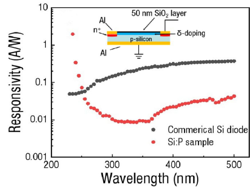
effect transistors, deep UV photodetectors, quantum devices and others. In this work, we formed a delta-doping layer in silicon by employing the flash lamp annealing to treat the PCl3 monolayers grafted on silicon surfaces. The delta-doping layer is atomically thin (<1nm). Low temperature Hall measurements show that the deltadoping layer is in metallic state and exhibits a weak localization phenomenon, implying that a two-dimensional electron gas is formed. When we form such an n-type deltadoping layer on a highly doped p-type Si substrate, a highly sensitive solar-blind UV photodetector is created, which traditionally was only possibly by using wide bandgap semiconductors such as gallium nitride (GaN) or silicon carbide (SiC).
References
[1] Gossmann, H. J.; Schubert, E. F. Delta Doping in Silicon. Critical Reviews in Solid State and Materials Sciences 1993, 18, 1-67.
[2] Popovic, R. S.; K. S.; Falk, U.; Stoessel, Z. A Silicon Ultraviolet Detector. Sensors and Actuators 1990, 553-558.
[3] Andrew, C. G.; Wood, A. G. O. N. Channel Profile Engineering of MOSFETs Using Delta Doping. Materials Research Society 1991, 220, 465.
[4] Yokogawa, T.; Takahashi, K.; Kusumoto, O.; Uchida, M.; Yamashita, K.; Kitabatake, M. 4H-SiC Delta-Doped Accumulation-Channel MOSFET. Materials Science Forum 2002, 389-393, 1077-1080.
WELCOME TO CHINA TO ATTEND THE ICANS
23-26 August, Nanjing, China
Connect with us:


