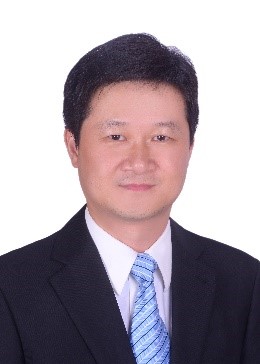
Xinbo Yang
Solar Cells
Soochow University,688 Moye Road, Suzhou, China
Email: xbyang@suda.edu.cn
Biography
|
Dr. Xinbo Yang, Jiangsu Distinguished Professor, is now with the College of Energy, Soochow University. He holds a Ph.D. degree from the Shanghai Institute of Ceramics, Chinese Academy of Sciences in 2010. From 2010 to 2020, he was a JSPS Fellow in Tohoku University (Japan), an ARENA Fellow in the Australian National University and a research scientist in the King Abdullah University of Science and Technology. His research interest is focused on the solar energy materials and solar cells, especially high efficiency silicon solar cells with passivating contacts and perovskite/silicon tandem devices. He has published more than 80 papers in peer reviewed journals and authorized 5 patents, presented 10 oral presentations on IEEE PVSC, EUPVSEC and PVSEC conferences, and involved seven PV projects in Japan, Australia, Saudi Arabia and China as PI or key members. |
|
|
Abstract for Presentation
The Progress and Future Prospects of Wide Bandgap Metal Compound-Based Passivating Contacts for c-Si Solar Cells
Advanced doped silicon layer-based passivating contacts (e.g. HJT and TOPCon) have boosted the power conversion efficiency (PCE) of single-junction crystalline silicon (c-Si) solar cells to over 26% [1-2]. However, the inevitable parasitic light absorption of doped silicon layers impedes further PCE improvement. To this end, alternative passivating contacts based on wide bandgap metal compounds (so-called dopant-free passivating contact, DFPCs) have attracted great attention, thanks to their potential merits in terms of parasitic absorption loss, ease-of-deposition and cost [3]. Intensive research activity has surrounded this topic with significant progress made in recent years. Various electron-selective and hole-selective contacts based on metal compounds are successfully developed, and high PCEs of over 23% were achieved on c-Si solar cell with MoOx and TiOx based carrier-selective contacts. In this work, we review the fundamentals and development status of DFPCs, and discuss the challenges and potential solutions in enhancing the carrier selectivity of DFPCs and device performance. Based on comprehensive and in-depth analysis and simulations, we point out the improvement strategies and future prospects for DFPCs design and device implementation.
We concluded that several improved demonstrations would need to be made before it could be considered as a serious contender for mainstream silicon PV industry. The first of these is the demonstration of a transparent electron contact without the need of a-Si:H passivation interlayer, which is highly desirable for PERC, TOPCon, SHJ and c-Si based tandem solar cells. To this end, increase the electron conductivity of the ESC (e.g., TiOx) by composition tuning (e.g., doping) and develop low WF TCO capping layer with negligible deposition damage (e.g., ZnO based TCOs deposited by ALD) are proven to be critical (Figure 1a). Similarly, the hole conductivity of HSC (e.g., NiOx) and the WF of TCO capping layer have to be increased for better hole selectivity (Figure 1b). Secondly, the long-term stability and process compatibility of DFPCs on the device level have to be demonstrated, which was rarely discussed in the previous reports. Given the fast development of this sub-topic, it is likely that such bottlenecks will be overcome in the coming years, and in doing so the performance gap between DFPCs and state-of-the-art doped silicon passivated contacts will continue to shrink.
References
[1] T.G. Allen, J. Bullock, X.B. Yang, A. Javey, S. De Wolf, Nat. Energy 2019, 4, 914.
[2] M. Hermle, F. Feldmann, M. Bivour, J. C. Goldschmidt, S. W. Glunz, Appl. Phys. Rev. 2020, 7, 021305
[3] J. Melskens, B. H. Loo, B. Macco, L. E. Black, S. Smit, W. M. M. Kessels, IEEE J. Photovoltaics 2018, 8, 373.
WELCOME TO CHINA TO ATTEND THE ICANS
23-26 August, Nanjing, China
Connect with us:


