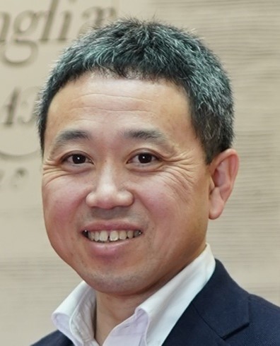
Keisuke Ohdaira
Silicon Thin Film
Japan Advanced Institute of Science and Technology
1-1 Asahidai, Nomi, Ishikawa, Japan
Email: ohdaira@jaist.ac.jp
Biography
Current research topics are related to formation of polycrystalline silicon films by flash lamp annealing and its application to thin-film solar cells, silicon-based solar cells including surface passivation of crystalline silicon using thin films formed by catalytic chemical vapor deposition (Cat-CVD), potential-induced degradation (PID) of n-type crystalline silicon photovoltaic modules, utilization of Cat-CVD silicon-based films for perovskite and perovskite/silicon tandem solar cells, and the development of novel encapsulant-free photovoltaic modules.
Abstract for Presentation
Formation of polycrystalline silicon films on glass substrates by flash lamp annealing of amorphous silicon films
Polycrystalline Si (poly-Si) films on glass substrates are expected for the usage in low-cost thin-film solar cells. We have thus far demonstrated that micrometer-order-thick precursor amorphous Si (a-Si) films can be crystallized by flash lamp annealing (FLA), millisecond-order annealing using pulse light from a Xe lamp.[1] Figure 1 shows a photograph of our FLA system. The crystallization of a-Si films takes place through lateral explosive crystallization (EC), continuous crystallization driven by the release of latent heat through phase transition from metastable a-Si to stable crystalline Si and its thermal diffusion to surrounding a-Si.[2] Recently, we have demonstrated that the EC of a-Si films induced by FLA can occur also on textured glass substrates.[3] The textured surface of glass substrates realizes the crystallization of a-Si films without film peeling even with no metal adhesion layer such as chromium. The textured surface of glass substrate may also enhance light trapping particularly when the poly-Si films are used for superstrate-type solar cells. In the presentation, I will review our previous achievements for the EC of a-Si films by FLA and also show our recent results for the formation of poly-Si films on textured glass substrates.
Figure 1. Photograph of the FLA system.
References
[1] K. Ohdaira, Y. Endo, T. Fujiwara, S. Nishizaki, and H. Matsumura, Jpn. J. Appl. Phys. 2007, 46, 7603.
[2] K. Ohdaira, T. Fujiwara, Y. Endo, S. Nishizaki, and H. Matsumura, J. Appl. Phys. 2009, 106, 044907.
[3] Z. Wang, H. T. C. Tu, and K. Ohdaira, Jpn. J. Appl. Phys. 2022, 61, SB1019.
WELCOME TO CHINA TO ATTEND THE ICANS
23-26 August, Nanjing, China
Connect with us:


