Guodong Yuan
Silicon Thin Film
Institute of Semiconductors, CAS, China
Qinghua East Rd.35, Haidian District, Beijing
Email: gdyuan@semi.ac.cn
Biography
Dr. Guodong Yuan is a professor in Institute of Semiconductors, CAS, China. He got his Ph. D degree in 2006 from Zhejiang University. After that, Dr. Yuan pursued his postdoc position in City University of Hongkong from 2006 to 2009. His research area includes silicon nanowire Field-Effect Transistors and applications in gas sensors. From 2009 to 2011, Dr. Yuan continued his postdoc research in Ruhr University Bochum Germany and Humboldt University Berlin in Germany. His research mainly include silicon nanostructures and applications in thermoelectric. In 2012, he joined Institute of Semiconductors, CAS, China. His present research area includes silicon MOSFET in cryogenic applications and quantum transport properties. He has published more than 90 papers in IEEE Tran. Electron Dev., Adv. Mater., Nano Lett. Etc.
Abstract for Presentation
Cryogenic mobility enhancement in Si MOS devices via SiO2 regrowth
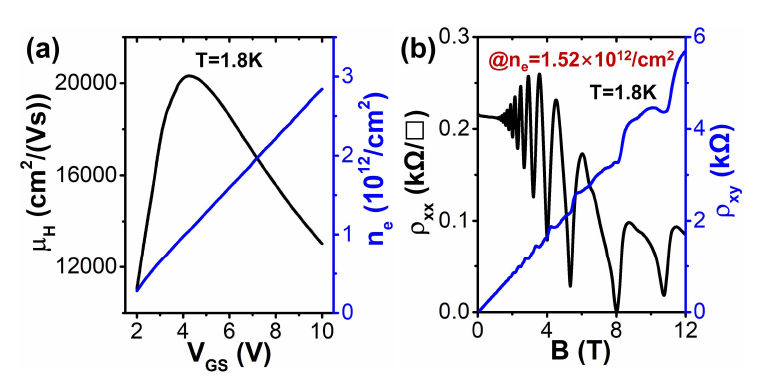
Cryogenic mobility enhancement, corresponding to the reduction of interfacial disorder, is always a research focus in Si-based MOS device manufacturing toward practical quantum computing chips. In this work, we report the dependency of MOSFET cryogenic mobility on reactive ion etching (RIE)-induced damages at 5-75K. We discover that RIE will introduce a lot of atomic steps and charged traps at SiO2/Si interfaces or conducting channel boundaries during the mesa formation stage, severely degrading device mobility, especially at a low temperature. With a post-RIE high temperature SiO2 regrowth process, the device cryogenic (1.8K) peak mobility is enhanced to ~20314 cm2/Vs at a small electron density of 1.05×1012cm-2, meaning the successful removal of RIE-induced extra effective scattering centers within the optimized device. Notably, our work presents the adverse impacts of RIE on MOS device cryogenic mobility and provides a feasible integration flow to recover device performances, which may promote the evolution of Si-based MOS quantum dot computation.
Figure 1. Magneto-transport properties of Si MOS devices. (a) Gate-controlled 2DEG hall mobility and density. (b) ρxx and ρxy properties as a function of magnetic field.
References
[1] S. Zhao, G. Yuan*, Q. Zhu, L. Song, D. Zhang, Y. Liu, J. Lu, W. Han, J. Luo*, IEEE Tran. Electron Dev. 69 (2022) 2585.
WELCOME TO CHINA TO ATTEND THE ICANS
23-26 August, Nanjing, China
Connect with us:


