Daniel Moraru
Silicon Thin Film
Shizuoka University
3-5-1 Johoku, Hamamatsu, Japan 432-8011
Email: moraru.daniel@shizuoka.ac.jp
Biography
|
· 2015~ Associate Professor, Faculty of Engineering, Dept. of Electronics and Materials Science & Research Institute of Electronics, Shizuoka University, Japan · 2012~2014: Assistant Professor, Research Institute of Electronics, Shizuoka University · Dr. Eng. (2007)
Daniel Moraru is working on the development of a unique research direction for semiconductor nanoscale devices, aiming for atomic- and molecular-scale electronics by utilizing dopant atoms (or “molecules”) in silicon. Through such research, he and his group are contributing to the advancement of a field coined as “dopant-based electronics”. Research studies are performed in a wide range, from fundamental simulations of atomistic effects to semiconductor-device fabrication at nanoscale and electrical characterization at single-electron tunneling level.
> 60 scientific papers in international journals & 3 book chapters > 300 contributions to international and domestic conferences Selected Awards:
|
Abstract for Presentation
Transport of electrons one by one through dopants in thin-Si devices
Electronics has been progressing at a fast, but steady pace over many decades along the Moore’s law: making devices smaller and smaller by various breakthroughs in technology and engineering, and by finding innovative ways to couple them into complex circuits. The limits of Moore’s law and the need for new physics to incorporate in future devices have attracted increased interest in alternatives beyond nanoscale miniaturization.
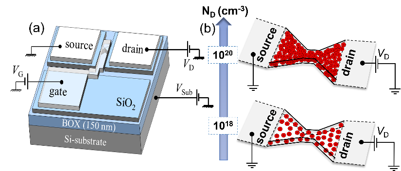
In our lab, we have pursued a new direction of research into atomic- and molecular-scale electronics using dopant atoms (or “molecules”) in silicon: dopant-based electronics.1 This is based on the well-established platform of silicon nano-devices but changing the active unit in transport to be the dopant-atoms substitutionally embedded in the Si crystalline matrix. Along this approach, we fabricate, characterize and simulate ultimately-small Si devices (with dimensions on the order of 10 nm) as schematically shown in Fig. 1(a), looking for signatures induced by such dopant-atoms in different regimes of dopant concentration [see Fig. 1(b)]. We will report single-electron tunneling (SET) in silicon-on-insulator nanodevices via individual donors2-4 or via clusters of donors5-8 working as quantum dots, not only in transistors, but also in tunnel diodes.9
Recently, we reported for the first time room-temperature single-electron tunneling in highly-doped silicon-on-insulator field-effect transistors, with channels patterned to have nanoscale dimensions. In such nano-channels, due to the random distribution of donor-atoms, we can identify devices in which clusters of a few donors form quantum dots with barriers sufficient high to sustain SET operation even up to T=300 K.10 These results are promising to demonstrate such fundamental mechanisms under practical conditions, bridging a pathway towards applications.
Fig. 1. (a) Schematic representation of a SOI-FET under bias. (b) Nanoscale channels doped with P-donors in a wide range of dopant concentrations.
References
[1] D. Moraru et al., Nanoscale Res. Lett. 6, 479-1-9 (2011).
[2] M. Tabe, D. Moraru et al., Phys. Rev. Lett. 105, 016803 (2010).
[3] E. Hamid, D. Moraru et al., Phys. Rev. B 87, 085420 (2013).
[4] A. Samanta, D. Moraru et al., Sci. Rep. 5, 17377 (2015).
[5] D. Moraru et al., Nanoscale Res. Lett. 10, 372 (2015).
[6] D. Moraru et al., Sci. Rep. 4, 6219 (2014).
[7] A. Samanta, et al., and D. Moraru, Appl. Phys. Lett. 110, 093107 (2017).
[8] A. Afiff, et al., and D. Moraru, Appl. Phys. Express 12, 085004 (2019).
[9] G. Prabhudesai, et al., and D. Moraru, Appl. Phys. Lett. 114, 243502 (2019).
[10] T. T. Jupalli, et al., and D. Moraru, Appl. Phys. Express 15, 065003 (2022).
WELCOME TO CHINA TO ATTEND THE ICANS
23-26 August, Nanjing, China
Connect with us:


